- Products
- Toys
- Schools
- Industry and Universities
- Maker
- Apps and Software
- Service
- Home
- Schools
- Learning material
- STEM Electronics
Making the basics of electronics understandable and sustainable!
Discover the exciting world of electronics with our STEM Electronics! Step by step, this construction kit teaches the basics of electronics and offers a wide range of different electronics topics. From simple to complex models, such as interchangeable indicators, many exciting functional models can be constructed with this construction kit. Teachers will find information material on the topic as well as ready-made tasks and solutions in our e-learning area.

Nach dem der italienische Physiker Alessandro Graf von Volta im Jahr 1800 die Batterie erfand, stand erstmals eine brauchbare Spannungsquelle zur Verfügung. Die Erforschung der Elektrizität nahm durch die zuverlässige Bereitstellung von Elektrizität richtig Fahrt auf.
1873, ein Dreivierteljahrhundert später, konnte Willoughby Smith die photoelektrischen Eigenschaften von Selen nachweisen. Nur ein Jahr später entdeckte Ferdinand Braun die gleichrichtende Wirkung von Halbleitern. Diese beiden Entdeckungen können als Geburtsstunde der Elektronik gelten.
In der ersten Hälfte des letzten Jahrhunderts war die Elektronenröhre das einzige aktive Bauelement der Elektronik. 1904 stellte John Ambrose Fleming eine Vakuum-Diode vor. Durch das zufügen von Steuergittern in den Elektronenstrom wurden in den folgenden Jahren immer weiter verbesserte Verstärkerröhren verfügbar. Eine Besonderheit dieser Technik waren sicher die Bildröhren (Ferdinand Braun, 1897). Sie wurden für Fernsehgeräte bis in die 2010er Jahre produziert. Ein weiterer besonderer Röhrentyp ist auch heute aus keinem Haushalt wegzudenken: das Magnetron für Mikrowellenherde.
Julius Edgar Lilienfeld ließ sich 1925 ein elektronisches Bauelement patentieren, das mit den heutigen Feldeffekttransistoren vergleichbar ist. Eine praktische Anwendung gelang nicht. Die technischen Voraussetzungen zur Herstellung waren einfach noch nicht gegeben.
John Bardeen, Walter Brattain und William Shockley aus den Bell Laboratories stellten 1947 den ersten Transistor vor und erhielten dafür 9 Jahre später den Nobelpreis für Physik.
In den folgenden Jahren wurde insbesondere die Herstellungstechnik von Transistoren immer weiter verbessert. In den 1950er und 1960er Jahren musste das anfänglich verwendete Germanium dem Silizium weichen. Silizium ist einfacher zu beschaffen, einfacher zu handhaben und damit preiswerter. Zeitgleich hat der Transistor die Röhre immer weiter verdrängt.
Jack Kilby entwickelte 1958 den ersten integrierten Schaltkreis (IC). Es handelte sich um ein FlipFlop aus 2 Transistoren. Heute werden mehr als 50 Milliarden Transistoren auf einem Chip vereinigt. Geschaltet wird mit Geschwindigkeiten im Gigaherz-Bereich.
Ab 1960 leiteten die MOSFETs (Metall-Oxyd-Halbleiter-Feldeffekt-Transistoren) die moderne Leistungselektronik ein. Eine Weiterentwicklung sind die IGBTs (Isolierte-Gate-Bipolar-Transistoren). Sie vereinigen die Eigenschaften von Feldeffekt- und bipolaren Transistoren. Es lassen sich Spannungen über 6000 Volt, Ströme bis weit über 3000 Ampere und Leistungen bis zu 100 Megawatt leistungslos durch geringe Steuerspannungen schalten.
Elektronik hat auch bei fischertechnik Tradition. Bereits 1969 brachten die fischerwerke ihren ersten Elektronik-Baukasten auf den Markt. Ziel war der praxisnahe Einstieg in die Elektronik. Viele weitere Experimentier- und Modellkästen bis hin zum Computing folgten bis heute.
Current and voltage
Task 1:
Every electronic circuit requires a supply voltage. This voltage is provided by a voltage source. The strength of the voltage source is expressed by the voltage applied to its poles. The voltage is a physical quantity with the formula symbol U. The level of the voltage is specified in the unit volt (V). The voltage of the battery used here in the battery holder is 9 volts.
In the battery, positive and negative charge carriers are separated by chemical processes. The negative charge carriers are the electrons. Positive charge carriers are places from which the electrons have been displaced.
The more electrons are separated from their positions, the higher the voltage. The voltage is the force exerted by the electrons between the poles. The voltage can be measured between the two poles of a voltage source.
If a closed circuit is connected between the two poles of the battery, the electrons can balance each other out via the circuit. A current flows through the circuit. The voltage drives the current through the circuit. The higher the voltage, the greater the current.
The current has the formula symbol I. Its magnitude is given in amperes (A). In electronic circuits, the flowing currents are usually very small. They are in the milliampere range (1 mA = 0.001 A). Even the fischertechnik XS motor used only "draws" around 100 mA from the voltage source under normal load.
The relationship between voltage and current is discussed in more detail in the next section.
Another important physical quantity is power. A circuit is always a sequence of obstacles for the current. Work must be performed on each component (including cables, plugs, switches, etc.) in order to overcome the obstacle. The work performed can often be observed directly. In our circuit, for example, this is the lighting of the LED. But the rotation of a motor or the heating of components also represent work performed. The work that can be done per unit of time is the power.
The power can be easily calculated:
P = U x I Power = voltage x current
Electronic components are sensitive to temperature. Strong heating can lead to changes in properties or even destruction of the component. For this reason, data sheets always state the maximum power dissipation.
The resistance
Task 4
The resistor is a passive component in electrical engineering and electronics. It causes a certain current to flow at a given voltage. The electrical resistance R is the physical quantity of a resistor. It is given in ohms (Ω). The dependence of voltage and current on an electrical resistor is proportional and is expressed by Ohm's law.
R = U / I Resistance = voltage / current
U = R * I Voltage = resistance x current
I = U / R Current = Voltage / Resistance
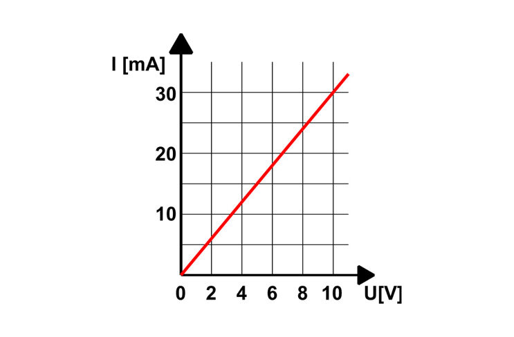
Current and voltage in a resistor are proportionally dependent on each other. The dependency can be represented in a characteristic curve. The figure shows the characteristic curve of a 330 Ω resistor. A current of 0.027 A or 27 mA flows at 9 volts. The characteristic curve of a resistor is a straight line. It is linear.
Figure Circuit symbol and characteristic curve
The electrical resistance of a component is always dependent on environmental conditions (e.g. temperature). In many electronic circuits, the influences are so small that they can be neglected. There are components in which the influences are specifically exploited. Due to the physical properties of the materials used, they react very sensitively to light (LDR = light-sensitive resistor) or temperature (NTC = thermistor or PTC = PTC thermistor), for example.
The resistors used in this box have the SMD (Surface Mounted Device) design commonly used today and are made from a ceramic carrier to which a metal or carbon film is applied. Resistors can also be realized using wire windings or semiconductor materials. The latter are used in integrated circuits.
Series connection of resistors
Task 5
If resistors are connected in series, their electrical resistances add up.
R = R1 + R2 + R3 + ...
Total resistance = resistor 1 + resistor 2 + resistor 3 + ...
If a voltage source is connected, a voltage proportional to the electrical resistance drops across each resistor. We speak of a voltage divider. Voltage dividers can be found everywhere in electronic circuits. Only voltage dividers make it possible to operate electronic components in their optimum working ranges. This is referred to as setting the operating point.
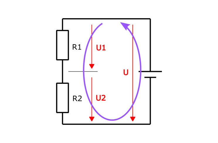
The illustration shows a voltage divider consisting of two resistors. The applied supply voltage U is divided into U1 and U2 at the two resistors according to their size. The relationship can be expressed in a formula:
U1/U2=R1/R2
If we look at all the voltages in the circuit diagram, we can also see the relationship between the supply voltage U and the partial voltages at the resistors. Since the voltage U is the same as the total voltage U1 and U2, the following formula results:
U = U1 + U2
This gives the ratio to the supply voltage
U/U2=(R1+R2)/R2
If the resistances are known (e.g. R1 = 47 kΩ, R2 = 3.3 kΩ), we can calculate U2, for example:
U2 = (U x R2)/(R1+ R2) = (9V x 3.3 kΩ)/(47 kΩ + 3.3 kΩ) = 0.59 V
We can also understand the circuit diagram in the figure as a network of voltages. The relationship is expressed by Kirchhoff's second law (mesh rule):
The sum of all voltages in a network is zero.
The rule can be understood with the help of the directional arrow for the mesh circulation. If you follow the entire circuit or network in an anti-clockwise direction, it becomes clear that the direction arrow for the supply voltage U points in the opposite direction to the direction of circulation. The voltage U must therefore have a negative sign. This confirms the rule:
U1 + U2 - U = 0.
Parallel connection of resistors
Task 6
If resistors are connected in parallel, their electrical conductance values add up (formula symbol G). The conductance expresses how well a material conducts electrical current. The conductance is the reciprocal of the electrical resistance. With this knowledge, a parallel connection of resistors can be calculated.
1/R= 1/R1+1/R2+1/R3+⋯
The total resistance R is always smaller than the smallest resistance of the parallel circuit.
If a voltage source is connected, the same voltage is applied to all resistors in the parallel circuit. A current flows through each resistor, which is inversely proportional to the electrical resistance (proportional to the conductance).
The figure shows a parallel circuit consisting of two resistors. The total current I flowing through the two resistors is divided into I1 and I2 according to their size. The relationship can be expressed in a formula:
I1/I2=R2/R1
If we look at all the currents in the circuit diagram, we can also see the relationship between the total current I and the partial currents through the resistors. Since the total current I is exactly the same as the sum of the currents I1 and I2, the following formula results:
I = I1 + I2
If the supply voltage and the resistors are known (e.g. U = 9 V, R1 = 47 kΩ, R2 = 3.3 kΩ), we can calculate the currents using Ohm's law:
I1 = U/R1 = 9V/(47 kΩ) = 0.19 mA I2 = U/R1 = 9V/(3.3 kΩ) = 2.73 mA
I = I1 + I2 = 0.19 mA + 2.73 mA = 2.92 mA
We can also understand the circuit diagram in the figure as a network of currents. The relationship is expressed by Kirchhoff's first law (node rule):
In a node of a network, the sum of all incoming currents is equal to the sum of all outgoing currents.
If you look at the node drawn in the circuit diagram, I flows into the node and I1 and I2 flow out of the node.
I - I1 - I2 = 0.
Capacitor
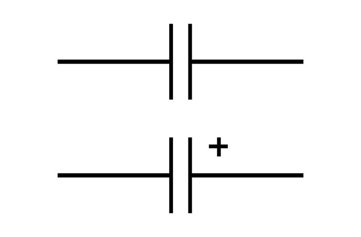
A capacitor can store electrical energy. In principle, it consists of two conductive plates that are separated by an insulator. The insulator is called the dielectric. The plates and dielectric can be made of a wide variety of materials. One example is the film capacitor. Two plastic foils and two metal foils are placed on top of each other and rolled up or folded. Each metal foil is given a connection that later protrudes from the enclosing housing.
Another important design is the electrolytic capacitor or electrolytic capacitor. The dielectric is formed by an insulating oxide layer. Electrolytic capacitors are polarized components. Incorrect polarity leads to destruction.
If the capacitor is connected to a voltage source, charge carriers flow onto the plates. The capacitor is charged. If the capacitor is disconnected from the voltage source, the charge is retained. However, the charge of common capacitors is so low that it cannot be used to operate electrical consumers. An LED would only light up briefly. Very low currents flow in electronic circuits. Here, the charge of capacitors is sufficient for many tasks. In the experiment on the capacitor, it is slowly discharged via high resistances to illustrate the effect.
Semiconductor
Modern electronics are based on semiconductor components. These components are based on high-purity semiconductor crystals. The crystals are deliberately contaminated with suitable substances. This is known as doping. Further doping with other substances is carried out at the required points in the crystal (redoping) in order to achieve the desired properties of the component.
There are two types of doping. With n-doping, atoms that have one electron too many (e.g. phosphorus, P) are incorporated into the crystal. These excess electrons can move freely. With p-doping, atoms with one electron too few are incorporated (e.g. boron, B). The places where electrons are missing are called holes or defect electrons. These sites also ensure conductivity in the crystal. Electrons can move from hole to hole. The boundary between the p-doped and n-doped regions is called the pn junction.
The conductivity of the crystal increases significantly as a result of the doping. The electrons have nothing better to do than fill the holes. They diffuse into the p-doped zone and recombine with the holes. The holes disappear, they seem to diffuse into the n-doped zone.
This is successful up to a certain depth (diffusion length) of the material. The process quickly comes to a standstill because the migration of the charge carriers creates an electric field that counteracts this process. An equilibrium is established. This zone without free charge carriers around the pn junction is referred to as the barrier layer or space charge zone. Due to the lack of charge carriers, current flow is no longer possible. The resulting electric field causes the diffusion voltage. For silicon, this is around 0.7 volts.
The diffusion voltage must be exceeded by applying an external voltage so that a current can flow through the semiconductor. The p-zone must be more positive than the n-zone. This means that the technical current direction in a pn junction always runs from p to n and therefore corresponds to the direction of movement of the holes. The electrons therefore move from n to p when current flows.
Diode
Tasks 7 and 8
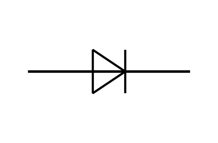
The diode is one of the simplest semiconductor components. It consists of only one pn junction. Usually, a p-type doping is introduced into an n-type doped semiconductor crystal at one point. Both zones are led out of the housing through connections. The connection at the p-zone is referred to as the anode, the connection at the n-zone as the cathode.
If a silicon diode is used in a circuit, there are two possibilities.
The anode is more positive than the cathode or vice versa. If the anode voltage is more positive by approx. 0.6 - 0.7 volts, the diode is operated in the forward direction. The diffusion voltage is reduced, electrons and holes dissolve their recombination and act as free charge carriers. A current flows.
In the opposite case, the electric field of the junction and the applied voltage act in the same direction. The electric field is further strengthened by the external voltage, the diode blocks and no current can flow. The diode is operated in the reverse direction.
If the voltage is increased too far in the reverse direction, physical effects in the semiconductor cause an unwanted breakdown. A high current flows like an avalanche, destroying the diode. The breakdown voltages of the diodes used in the experiments are approx. 700 volts.
LEDs (light emitting diodes) are a special type of diode. When operated in the forward direction, they convert electrical energy into light. The forward voltage is 1.8 to 3.7 volts, depending on the material and light color. The reverse voltage is usually around 5 volts.
The transistor
Tasks 9 to 11
The "bipolar transistor" (BJT) or simply transistor is a semiconductor component with two junction layers. This means that there must be two pn junctions. The order of doping determines the electrical properties of the transistor. The figure shows the two possible combinations.
If a voltage is applied to a transistor between the base and emitter, the base current IB flows after the diffusion voltage is exceeded. The circuit behaves like a diode. A large number of charge carriers enter the base layer with the base current. As this is very narrow, more and more charge carriers have to escape into the junction between the base and collector. The charge carriers cause the barrier layer to degrade and become conductive. A collector current IC can flow. The strength of the current depends on the supply of charge carriers in the base. A current flows through the collector and emitter, which is dependent on the base current. Without a supporting base current, the process comes to a standstill. This does not happen abruptly, but takes a short time. The charge carriers must flow out of the base. This is the reason why a transistor cannot switch infinitely fast, it has a cut-off frequency. This places limits on fast applications, e.g. in computers. Another consequence: a transistor switches on much faster than it switches off.
The ratio between collector current IC and base current IB is the current amplification factor B. It is a parameter determined by the manufacturer. Depending on the type of transistor, the current amplification ranges from 5 to 1000. The current amplification of the transistors used in the experiments is around 200.
"Amplification factor B = " ("Collector current" "I" _"C" )/("Base current" "I" _"B" )
The transistor is a current amplifier. If the base current is increased, the collector current increases. At some point, the current is limited by the load resistor. Even if the base current is increased, the collector current cannot increase any further. The transistor is fully controlled. It is operated in saturation. This operating mode is used if the transistor is to be used as a switch.
If the transistor is used as an amplifier, it must be operated in a range in which the collector current is proportional to the base current.
Various voltages and currents are important in a transistor circuit. They are shown in the figure.
UB - Supply voltage
UBE - base-emitter voltage
IB - base current
UCE - collector-emitter voltage
IC - collector current
RL - Load resistor (e.g. a lamp)
RB - Base series resistor
B - current amplification factor
UCB and IE are only of minor importance. They can be calculated from the other values at any time.
Care must be taken to ensure that the transistor is operated within the manufacturer's specifications. The following parameters must not be exceeded:
UCB0 - Maximum collector-base voltage
UCE0 - Maximum reverse voltage
UEB0 - Maximum base-emitter voltage
IC - Maximum collector current
Ptot - Maximum power dissipation (UCE x IC, base current neglected)
Some parameters are represented by characteristic curves to express the dependence of different values on each other. The most important characteristic curve that describes a transistor is the output characteristic curve (figure on the right). The relationship between the collector-emitter voltage and the collector current can be read from it for different base currents. The amplification factor can also be calculated from the line of a base current after reading the collector current. The yellow line indicates the range that must not be exceeded. The product of collector-emitter voltage and collector current indicates the power converted into heat. This would be too high beyond the line and would destroy the transistor.
Many manufacturers no longer specify all characteristic curves. The parameters contained in the data sheet must then be used to calculate circuits. Transistor circuits can be calculated using the information from the data sheet. Only Ohm's law and Kirchhoff's rules are required for this.
If the resistance of a load (consumer) is fixed, the current through it and thus through the collector can be determined:
UL = UB - UCE, IL = IC = UL / R
The base current can be calculated by simply dividing the collector current by the current amplification factor B:
IB = IC / B
The required base current in turn determines the base series resistor. The voltage URB drops across this. The voltage corresponds to the supply voltage minus the diffusion voltage of the base-emitter path:
URB = UB - 0.7V
If this voltage is known, the base series resistor can be calculated:
RB = URB / IB
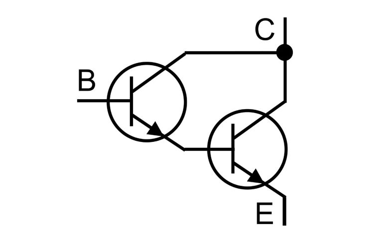
The Darlington circuit
Task 12
The Darlington circuit is a special interconnection of two transistors (see illustration). The base and collector currents that flow out of the transistor via the emitter are used directly as the base current for the second transistor. In this circuit, the current amplification factors of the two transistors are multiplied.
Btotal = BT1 x BT2
Darlington circuits have very high current amplification factors. Factors of over 500,000 are achieved.
If Darlington circuits are required, Darlington transistors are used directly today. They consist of a Darlington circuit in a transistor housing.
MOSFET
metal-oxyde-semiconductor-field-effect-transistor
Tasks 13 to 15
MOSFETs have replaced transistors in many areas. This component is used predominantly in digital and power electronics in particular. MOSFETs can be produced very efficiently in enormous quantities and combined into complex circuits on a single piece of silicon. There are microprocessors that consist of more than 50 billion individual MOSFETs.
In power electronics, MOSFETs are used to switch enormous currents at very high voltages. The use of mechanical power switches is no longer necessary. This is made possible by the very good electrical properties of modern MOSFETs.
In principle, the MOSFET is a semiconductor component that behaves like a voltage-controlled resistor. In contrast to a bipolar transistor, no control current flows. The MOSFET is controlled without power.
A MOSFET consists of a semiconductor crystal that can be weakly n- or p-doped. There are special types that are based on an undoped crystal.
An n-channel MOSFET, as used for the experiments, consists of a p-doped silicon (substrate) into which two n-zones are inserted (figure top left). The two zones are connected to the drain and source terminals. An insulating layer is applied to the area between the zones. The gate electrode is located on the insulating layer. The bulk connection is located on the substrate. This is connected internally to the source.
If a positive voltage is applied to the gate (bottom left figure), electrons are attracted by the resulting electric field. The gate behaves like a capacitor in relation to the substrate. The accumulated electrons form a channel below the gate electrode, which behaves like n-doped silicon. The channel connects the two n-zones with each other and removes the barrier layers. A current can flow. In modern MOSFETs, the channel has a very low resistance (< 10 mOhm). The power loss can therefore be kept very low, even with large currents.
The current flow between drain and source is possible in both directions. However, the manufacturers optimize the MOSFETs for the flow direction drain - source.
By connecting several MOSFET cells in parallel on a substrate, components can be realized that can switch considerable currents (> 3000 amperes).

The MOSFET as a switch
Task 14 to 15
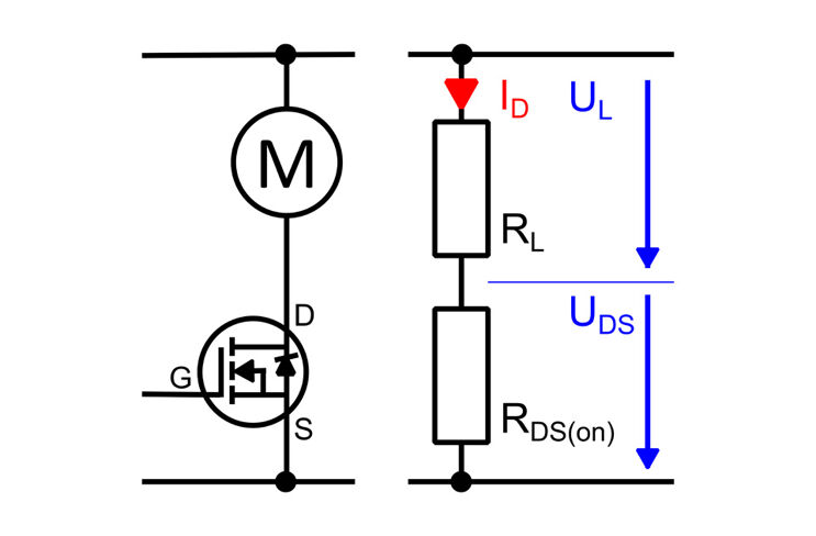
MOSFETs for power electronics should have the lowest possible resistance RDS(on) of the channel between drain and source. Today, values of a few milliohms are achieved.
The load current ID flows through the load resistor and channel between drain and source. The channel is connected in series with the load resistor RL. The illustration shows the connection in our circuit and as an equivalent circuit diagram. The aim is to make RDS(on) considerably smaller than RL. This ensures that only a very small part of the supply voltage drops across the MOSFET. The power that is converted into heat in the MOSFET remains low. The component does not heat up so much that it is destroyed.
There are parameters that describe the electrical properties of a MOSFET. They are determined by the manufacturing process. All parameters can be found in the manufacturer's data sheets.
UBR - Breakdown voltage of the drain-source path.
IDmax- Maximum current that may flow through the drain-source path.
RDS(on) - Resistance of the drain-source path when switched through.
UGSth - Threshold voltage from which the drain-source path conducts.
Ptot - Maximum power loss that is converted into heat in the semiconductor.
The above parameters are sufficient in power electronics to design circuits with MOSFETs. The range in which a MOSFET may operate is limited by the parameters.
It may ...
... not switch a voltage higher than UBR.
... no current greater than IDmax may flow.
... no power greater than UDS x ID may be converted.
... no current greater than UDS / RDS(on) may flow.
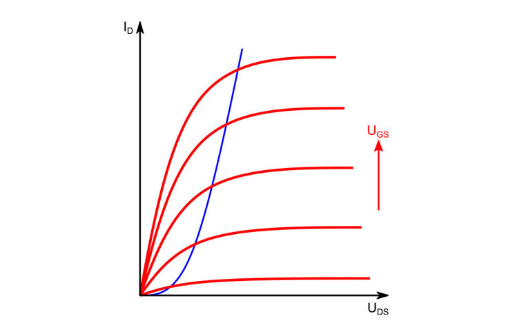
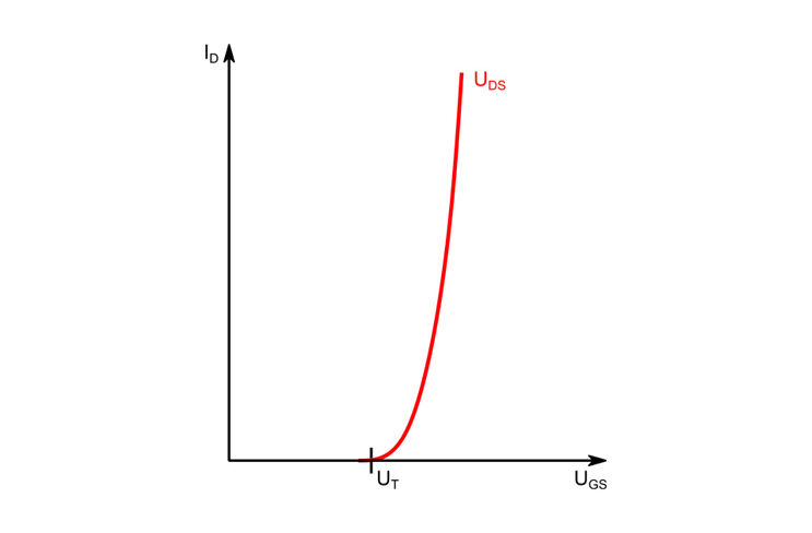
Some properties are published by the manufacturers in the form of characteristic curves. One of these characteristics is the transfer characteristic (top left). It indicates the influence of the gate voltage UGS on the drain current ID. Typically, the threshold voltage UT must be exceeded in order for a drain current to flow at all.
We use the characteristic curve to find out how high the gate voltage must be in order to reliably switch the desired current through the load.
The MOSFET used in the experiments has a particularly low threshold voltage. It is intended for direct use in logic circuits. These work with 3 to 5 volts.
Another characteristic curve is the output characteristic curve (bottom left). It provides information about the dependence of the drain current ID on the drain-source voltage UDS for several gate voltages UGS.
In switching mode, the area to the left of the blue line is of interest. In this area, the resistance of the drain-source path is most favorable.
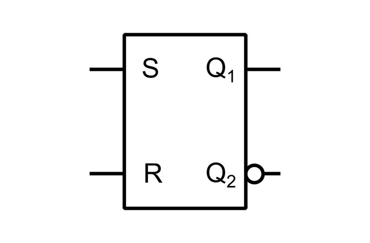
The bistable tilting stage
Task 17
The bistable flip-flop or bistable multivibrator is an important basic electronic circuit. In principle, it represents a memory location for one bit. This circuit is found in thousands of microprocessors and is the basic circuit for dynamic RAM components. The bistable toggle stage is also known as a flip-flop.
Today, bistable flip-flops are only built from individual transistors in exceptional cases. There is a large selection of integrated circuits that contain one or more of these circuits.
The following logic table shows the relationships between signals at the inputs and the two outputs. This is the simplest form of a bistable flip-flop, the RS flip-flop. The name is derived from the two inputs.
|
S |
R |
Q1 |
Q2 |
Remark |
|
1 |
0 |
1 |
0 |
Set (set) |
|
0 |
0 |
X |
X |
Last saved status |
|
0 |
1 |
0 |
1 |
Delete (reset) |
|
1 |
1 |
0 |
0 |
Only as long as a signal is present, cannot be saved |
The flip-flop often has two outputs. The second output is then negated. This means that the opposite logic signal is always present. The negation is indicated by the small circle.
If one of the two inputs is activated with a logic signal, this is forwarded to the output and stored. If there are no signals at the inputs, this state is retained. Only a signal at input R can reset the output. If both inputs are assigned signals, an undesired state is present. After removing the signals, the output remains set or deleted depending on the order in which it was switched off.
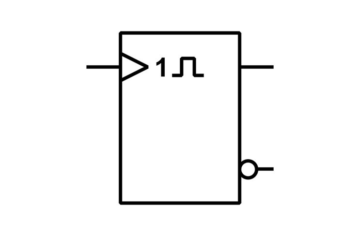
The monostable tilting stage
Task 18
The monostable tilt stage or monostable multivibrator is a basic electronic circuit with a time response. The time response is represented by the rectangular pulse in the circuit diagram (figure on the left). The circuit diagram also shows that the input does not require a voltage level but is switched from 0 to 1 by a pulse. This means that the transition from 0 (no voltage) to 1 (voltage applied) triggers the switching process. The transition is referred to as an edge. We speak of a dynamic input. The triangle in the circuit diagram represents a dynamic input. The monostable toggle stage is also referred to as a mono flop.
The mono flop often has two outputs. The second output is then negated. This means that the opposite logic signal is always present. The negation is indicated by the small circle.
If the input is activated with a logic signal, this is forwarded to the output and stored. After a preset time, the output automatically returns to the initial state.
The time period can be specified by an RC element. An RC element is a combination of resistor (R) and capacitor (C). A capacitor is charged or discharged via the resistor. A period of time is required for the process, which can be calculated using the following formula.
t=ln(2)*R1*C1
The logarithm ln(2) can be replaced by the constant 0.7.
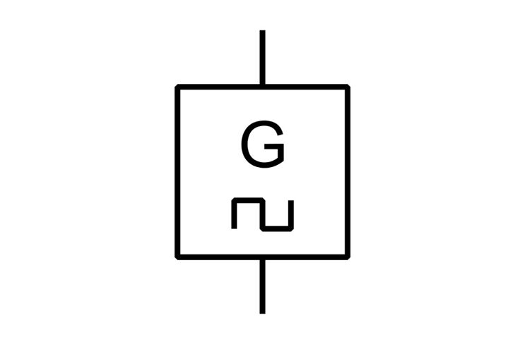
Astable tilting stage
Task 19
The astable tilt stage or the astable multivibrator is a basic electronic circuit that automatically switches periodically between two states. The switching times are determined by 2 RC elements.
There is no separate switching symbol for the astable tilting stage. In principle, it is a generator with a specific frequency. As the output voltage oscillates between two values, it is similar to a square wave generator.
A certain time T is required to run through a complete cycle. This is the sum of the times of the two RC elements. If both RC elements have identical dimensions, they are symmetrical. The following formula can then be applied. The constant 2 indicates that there are 2 identical RC elements.
T=2*ln(2)*R1*C1≈1,386*R1*C1
In practice, the period duration T is rarely specified. More important is the number of pulses emitted per time unit. The number of pulses per second is the frequency f. The unit of measurement for frequency is the heart rate (Hz). The frequency can be calculated using the following formula:
f=1/T
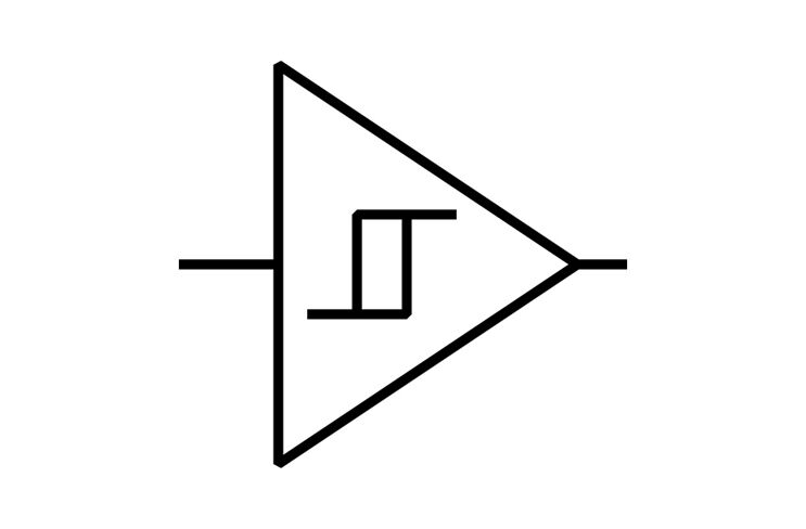
The Schmitt trigger
Task 20
The Schmitt trigger is a toggle circuit in which an input voltage is compared with a voltage specified in the circuit. A special feature of the Schmitt trigger is that the switch-on and switch-off voltages are not identical. The difference is called switching hysteresis or simply hysteresis.
The output voltage can be close to the supply voltage. The Schmitt trigger is suitable for converting any voltage into a defined logical output level.
The abrupt switching of the output voltage is achieved by the common emitter resistor RE. The emitter voltage of T2 is also increased by a voltage drop that occurs there as soon as T1 passes through a base voltage. At the same time, the base voltage of T2 decreases as T1 conducts. The voltage between the base and emitter of T2 drops abruptly, T2 blocks and the circuit is flipped.
The ability to deliver clearly defined output levels in particular makes the Schmitt trigger a very frequently used circuit. All signals that are transmitted through the real world are subject to interference. The transmission of digital information via satellite or long undersea cables would be impossible if Schmitt triggers did not restore the original signals.
This capability is illustrated in the figure below left. The voltage difference shown by the two black horizontal lines is the hysteresis. The switch-on voltage is always above the switch-off voltage.
The differential amplifier
Task 21
A differential amplifier is an amplifier circuit with two inputs. The voltage difference between the two inputs is amplified. Differential amplifiers are practically only available as complete circuits in the form of integrated circuits. Operational amplifiers are of great importance. They also consist of a differential amplifier in the input circuit. However, this is extended by many additional transistor stages in order to achieve the desired properties.
Differential amplifiers are very important as operational amplifiers and in measurement technology.
A simple differential amplifier consists of two transistor amplifiers which are coupled via a common emitter resistor. The emitter resistor should allow a constant current to flow independently of the control of the transistors. In industrial circuits, so-called constant current sources are integrated into the circuits.